While I enjoy the DIY thing, building a business requires a different mindset. I don’t want to cut out the creativity, but I also can’t afford to waste time. You’ll hear business types discuss the “opportunity cost” associated with something, and I can tell you it’s a very real thing.
For my possibly upcoming business, that means that I can’t afford the time to play with things like hotplate or toaster-oven reflow for PCB assembly. I don’t have the time to tinker. And so, for the first time, I decided to pay for professionals to do the job.
Enter JLCPCB.
Who Are They?
JLCPCB has been around for quite a while, and I’ve heard a lot of varying stories about them. The biggest thing is that they’re supposed to be very easy to work with, and very cheap. You send them the design and the Bill of Materials, and they send you back assembled boards.
They have a fairly good reputation; I’ve never heard anyone complain about anything showstopping. I figured, why not? I had (and have) far too much to do, and it wouldn’t hurt to give them a chance to build my prototypical toys.
I’ll say up front that I’m very happy with them, though as always, the devil is in the details.
The Design (And A Minor (But Positive) Rant About My EDA Tool Of Choice)
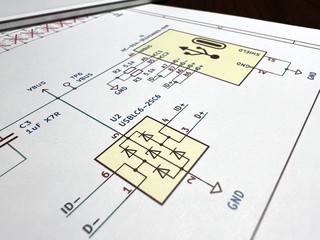 I won’t yet say what my actual product is, but I will tell you a few
things about the first bit of prototype hardware. It’s actually
fairly straightforward: an ESP32 (an S2 MINI-2 module in this case),
some LEDs, a USB connector, some buttons, and some support circuitry.
Nothing particularly troublesome, and certainly nothing outright
exotic.
I spent a few days designing both the initial schematic and the board layout in KiCad 7. Long ago I started out with Eagle (which is what my last board was designed with), and in my opinion, post-6.0 KiCad blows it out of the water. I’m extremely happy with the choice.
Of course, it’s not always trouble-free; I run macOS, and while there is a native Apple Silicon build that performs very well, it does sometimes have problems. In this case, a bug crept in that caused crashes under certain circumstances involving saving files and then trying to access the menu bar.
I cannot count the number of times I crashed it.
Fortunately the KiCad people are generally responsive, and someone else had long since pointed it out. I downloaded a release candidate for the next release, and the problem went away. Yay!
But I digress.
Once the schematic was done, it was onto the board. There is no design rules file that I know of for pulling in the various manufacturing constraints for JLCPCB, so I had to dig them out of the JLCPCB capabilities page and manually enter them in the board setup. The only trouble I had there is that I’m not an expert on this stuff, and I had to do my best at translating their terminology to KiCad’s.
I seem to have managed OK, though.
Of course, then I realized that I needed to specify the specific parts I was going to use for this, and that led down a different rabbit hole…
A Gotcha: The Parts
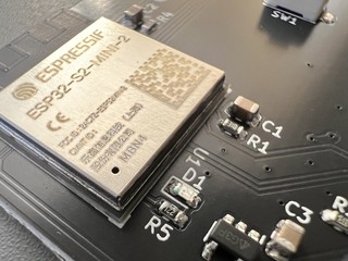 One thing about working with JLCPCB, is that you need to use their
parts library. This is a double-edged sword. You can probably find
what you need, but that’s not guaranteed, and if you can’t… well, I
could, so I really don’t know what might have happened.
Their page implies that they’ll send you partially-completed boards, and that did worry me. Luckily, it didn’t happen to me.
The bigger issue, though, is that there are two tiers of parts within their library: Basic and Extended. The former are mostly the simple things – resistors, capacitors, and overly common ICs that everybody uses. I think there are around seven hundred Basic parts.
Anything truly interesting is going to be an Extended Part, and that unfortunately includes any kind of ESP32 module.
Why is this bad? Cost, of course. The trick to the Extended Parts is that they charge you to mount the reels – $3 per part. That may not seem like a lot, but it does add up when you’re ordering in small quantities. And since a fair few of your parts are likely to be extended ones…
This is why I ordered ten of the prototype. The parts themselves (and even the boards and per-unit assembly cost) were cheap. The setup fees and the like were a different story. I ended up paying $15 for extended components.
More on the cost later.
The KiCad JLCPCB Plugin
Like all board houses, JLCPCB expects data in a certain format. Thankfully there’s a plugin available for KiCad that facilitates this. If you know how to deal with KiCad in general, then using it is a breeze.
For me, the steps were thus:
- Install the aforementioned plugin in KiCad (that and the Espressif library plugin were the only ones I used.)
- Add attributes to all instances of my parts indicating the JLCPCB part numbers to use.
- Click the button to generate the ZIP file to send to JLC.
And… that was it.
I did, of course, pull apart the zip file to see what was in it, and it’s what you would expect: the apprpriate gerbers under appropriate names, the drill file, the BOM, etc. I did have to go back and do a round or two to exclude a few things that I knew shouldn’t appear in the BOM (things like DNP components that I forgot to actually mark as “Do Not Place”).
With that done, I was able to simply upload the file to JLCPCB and start clicking away at options to order my boards.
I highly recommend the plugin. It made life very easy.
Board Choices
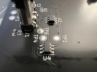 The board is roughly 3 inches square. It’s merely double-sided; I
had no reason to go for a four layer or greater board, especially not
for the prototype. All in all, just your basic board; nothing special.
Most of the important options I selected after uploading the files to JLCPCB were standard stuff. I used the default board composition and thickness (1.6mm); standard copper weight (1oz); and tented vias. All in all, nothing special in general.
Where I departed from “default” was with the lead-free HASL finish and the black solder mask. The latter is actually a product dictate rather than an aesthetic choice; I need the board to be black. Surprisingly, while the lead-free finish cost me a little extra, the solder mask only cost a bit of time. That’s a departure from the last time I had boards made…
Oh, and I specified the location of the order number they wanted to print on the board, rather than pay the $1.50 to remove it. It’s just a prototype anyway.
In the end, with applied coupons, the cost of the boards was $6.73 for ten of them; $0.43 of which was because I chose the option to allow me to confirm the production files. I’m paranoid like that, not that it really mattered in the end.
Assembly
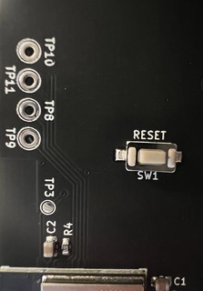 Ordering the assembly seemed fairly straightforward. They had my
files, they had my BOM and position/placement files, and life was
good.
In theory.
There was a bit of almost bait-and-switch going on here.
They like to advertise PCB assembly as free, but that only holds if you stay within a very specific lane. If you do anything at all outside of that lane, it’s no longer going to be free.
The big thing that got me was that I needed parts placed on both sides of the board. The instant you do double-sided assembly, you are no longer within their economy assembly envelope. Now you have to use their “standard” service, which is much more expensive.
I required parts placement confirmation, baking where required, and depanelization/removal of edge rails prior to shipment, that I can recall. The baking was due to the LEDs I was using; the datasheet specified that it was required.
That baking cost me seven and a half bucks in extra fees.
There was some other “advanced” option that I chose that cost me another four dollars in such fees, and I cannot for the life of me remember what it was – nor does it say anywhere that I can find. It’s just an “Advanced Option Fee”. This is annoying; I wish it was called out, since I didn’t note it at the time.
But back to the process.
Pre-Production
 Once the order is submitted, there’s a lot of hurry up and wait, as
one would expect. Their interface is actually pretty decent; it keeps
you fairly well informed of what’s going on. I waited for perhaps a
day or two before they asked me to confirm the production files for
the PCB, which I did.
My memory is not serving me well as to whether or not the PCB order went into production prior to component placement being confirmed for the assembly order. Either way, that process was fairly easy; they have an online system that allows you to specify the component placement adjustments (once you figure out how the interface works), and off you go. When they sent me the final position information for confirmation, it was all correct.
That was perhaps the most nerve-wracking part of the whole process. You have to go through and make sure that each part is in the proper place and has the correct rotation so that the pins are where they’re supposed to be. More than a dozen parts had to be adjusted in my case.
Why? Because every vendor has a different idea about how component orientation should be specified, and JLCPCB is no exception. You will probably deal with this with almost any assembly house. There’s supposed to be a standard, but it is… not followed well from what I understand.
Note that JLCPCB’s people will generally do this for you I believe. I’m just paranoid, as I mentioned, so I looked over their shoulders and confirmed everything. I found no problems.
The one issue that required interaction with them (via email in this case) was answering questions about the component baking. Once that was sorted out – yes, the LEDs needed to be baked – life was good. I only worked with their people via email, and had no issues; they communicated clearly.
Once that was done, it was off to the races.
Production
The production process is straightforward and easily monitored. You can watch as your board goes through the various phases (drilling, copper deposition, and on through a dozen other steps). My board took about a day to get through it all, and then went on to assembly.
There was a delay in the middle of all of this due to a weekend, but that’s not their fault.
They’re quite transparent; you can watch the production & assembly process proceed through each step. It went through very quickly, and soon enough was winging its way to me, courtesy of DHL.
The Result
Quite frankly, I’m shocked at how the prototypes came out.
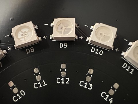
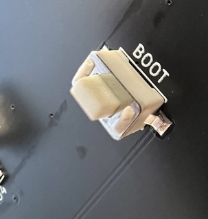
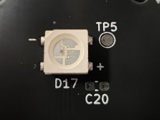
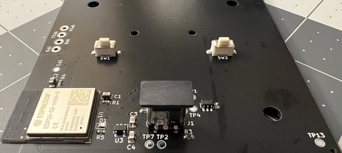
They’re exactly what I designed, and exactly what I envisioned, except better. As far as I’m able to assess such things, the quality is very high. I can’t spot any issues with the PCB, the parts, or anything. It all looks very professional; my only quibble was that the packing for shipping appeared slightly slapdash.
Much more importantly for me, though, the boards work, right out of the box. Or at least, the four that I’ve powered up so far have done, and a visual inspection suggests that the others will as well.
All in all, they produced a very solid product that took about ten days, cradle to grave. I ordered on February 19, and had the boards in my hand on March 1. I’m very happy with the result, and I will be using their service again.
Of course, we still have to discuss–
The Price
And this is where I have to rant slightly.
First, though, let me be clear: regardless of my forthcoming comments, it was a good deal IMO. The total in the end was just shy of $190 for ten units. That’s not bad considering the quality of the service, the low quantity, and that that number is all inclusive, including the cost of parts and shipping. So I really can’t complain too much overall.
That said…
Here’s the approximate cost breakdown in the end:
| Item | Cost |
|---|---|
| PCB (total, qty 10) | $ 6.73 |
| PCBA Setup Fee | $ 50.00 |
| Stencil | $ 15.71 |
| Components | $ 38.16 |
| Extended Compoments Fees | $ 15.09 |
| SMT Assembly | $ 3.41 |
| Packaging Fee | $ 0.47 |
| Supplemental Fees | $ 12.25 |
| Special Component Fee | $ 0.30 |
| Shipping | $ 42.63 |
| Sales Tax | $ 13.47 |
| Discount (from coupon) | $ -10.00 |
So all in all, just shy of $19 per unit. Now, as I said above, that’s a pretty good deal in the end for small quantity production. That said, I found myself kinda miffed at certain things.
First: the extended component fees. Since I’m already paying $50 in unexpected setup fees (remember, I expected “free” assembly when I started, based on their advertising!), I would expect that I wouldn’t pay additional setup fees just to load components.
That one I can get past, though; it’s understandable, along with all the other nickle-and-dime stuff that came with it. What I found kinda galling was the $7+ fee for baking the LEDs. Seriously, aren’t they just throwing them in an oven for a couple of days? This is not exactly a hardship IMO.
Really, it was the bait-and-switch feel with the economy vs standard assembly that annoyed me, though. I wouldn’t have complained even one jot if I hadn’t believed going in that I would get free assembly. I can understand some extra charges – an extra solder paste stencil, for example, since it’s a double-sided board – but…
Yeah. Rant over. I’m just annoyed that it cost twice what I expected.
In the end, it’s actually an incredible value. I really doubt that you could get anywhere close to this with a US-based manufacturer, unfortunately. Advanced Circuits, for example, are still charging $33 per board for two layer boards, with a minimum quantity of 3. So $99 base price, and for only three units instead of ten.
For just the PCB.
So yeah. JLC’s pricing is shockingly good, in the end. It just felt wrong. And the shipping for ten boards was a bit expensive; I’m actually very curious to know what it would cost to get, say, a thousand shipped.
Maybe I’ll find out some day.
Final Thoughts
In the end, I’m actually deeply impressed. If I had the millions of dollars I would expect it to take, I would be of a mind to try to build a competing service here in the US. I don’t even know if that’s possible, though.
The pricing is incredible, and that’s before you get to the parts pricing, which is also top notch as near as I can tell (though you do lose some of that savings with the extended component fees).
In the end, I have no room to complain. I will be using them again. There’s just no reason not to. At some point I may give PCBWay or one of the other players a shot just on general principle, but we’ll see.
P.S.: Sorry this took so long to get out. I’ve been very, very busy, and didn’t have time to write up a long post like this. I’ll try to do better… Watch the sidebar, too, since I may soon have other updates on non-featured things!
